Altera FPGA EP4CE10E22I7N Cyclone IV E 10320 Cells, 10320 Gates, 423936 bit 645 Blocks, 144-Pin EQFP
- RS Stock No.:
- 830-3502P
- Mfr. Part No.:
- EP4CE10E22I7N
- Manufacturer:
- Altera

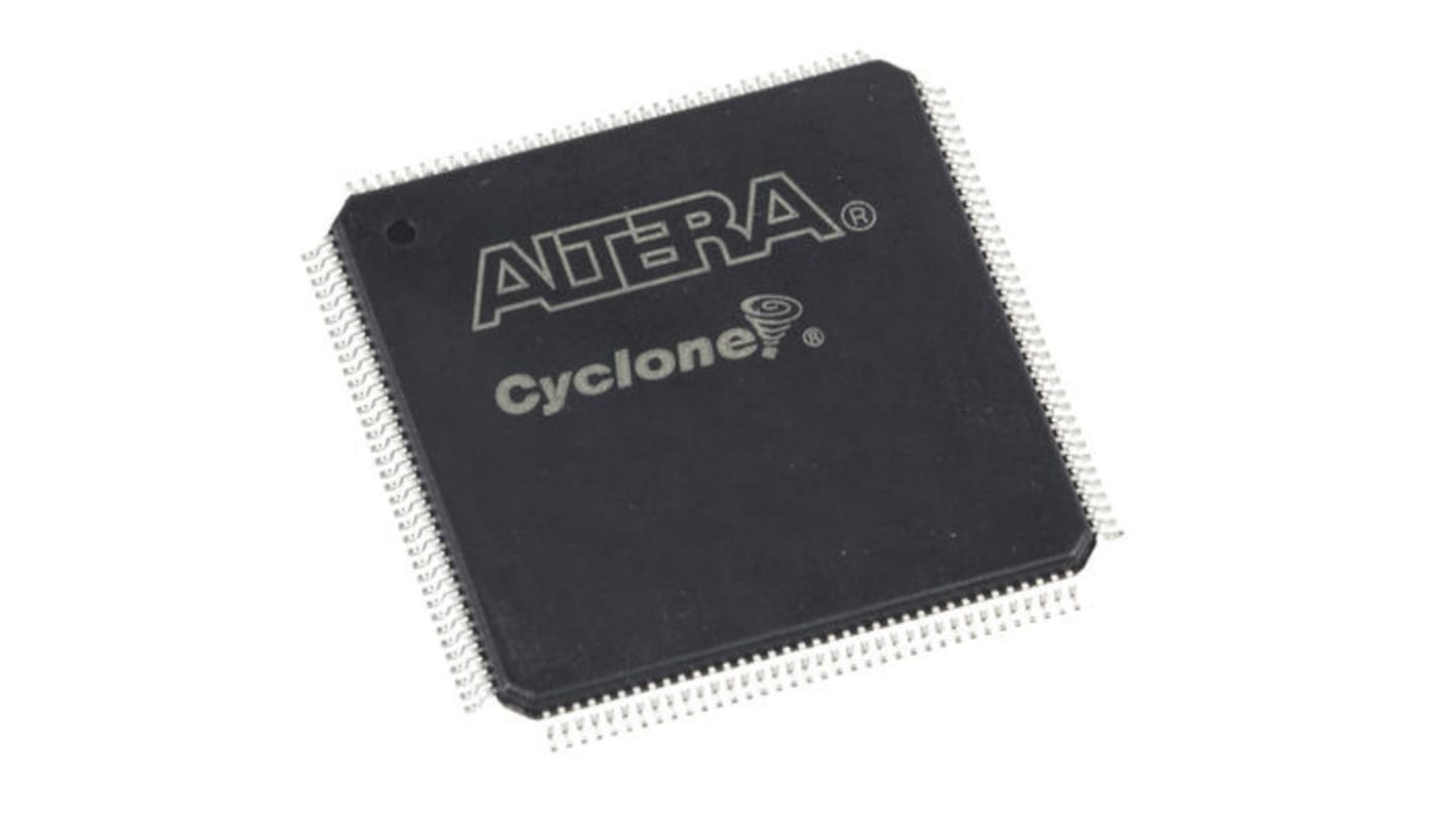
This image is representative of the product range
Currently unavailable
We don't know if this item will be back in stock, RS intend to remove it from our range soon.
- RS Stock No.:
- 830-3502P
- Mfr. Part No.:
- EP4CE10E22I7N
- Manufacturer:
- Altera
Specifications
Technical data sheets
Legislation and Compliance
Product Details
Find similar products by selecting one or more attributes.
Select all | Attribute | Value |
|---|---|---|
| Brand | Altera | |
| Product Type | FPGA | |
| Series | Cyclone IV E | |
| Number of Logic Gates | 10320 | |
| Number of Logic Cells | 10320 | |
| Number of Logic Units | 645 | |
| Number of Multipliers | 360 (18 x 18) | |
| Mount Type | Surface | |
| Package Type | EQFP | |
| Minimum Supply Voltage | 1.15V | |
| Maximum Supply Voltage | 1.25V | |
| Pin Count | 144 | |
| Number of RAM Bits | 423936bit | |
| Minimum Operating Temperature | -40°C | |
| Maximum Operating Temperature | 100°C | |
| Standards/Approvals | No | |
| Length | 22mm | |
| Automotive Standard | No | |
| Select all | ||
|---|---|---|
Brand Altera | ||
Product Type FPGA | ||
Series Cyclone IV E | ||
Number of Logic Gates 10320 | ||
Number of Logic Cells 10320 | ||
Number of Logic Units 645 | ||
Number of Multipliers 360 (18 x 18) | ||
Mount Type Surface | ||
Package Type EQFP | ||
Minimum Supply Voltage 1.15V | ||
Maximum Supply Voltage 1.25V | ||
Pin Count 144 | ||
Number of RAM Bits 423936bit | ||
Minimum Operating Temperature -40°C | ||
Maximum Operating Temperature 100°C | ||
Standards/Approvals No | ||
Length 22mm | ||
Automotive Standard No | ||
Cyclone FPGA, Altera
An FPGA is a semiconductor device consisting of a matrix of Configurable Logic Blocks (CLBs) connected through programmable interconnects. The user determines these interconnections by programming SRAM. A CLB can be simple (AND, OR gates, etc) or complex (a block of RAM). The FPGA allows changes to be made to a design even after the device is soldered into a PCB.
Related links
- Altera FPGA Cyclone IV E 6272 Cells 276480 bit 392 Blocks, 144-Pin EQFP
- Altera FPGA EP4CE6E22I7N Cyclone IV E 6272 Cells 276480 bit 392 Blocks, 144-Pin EQFP
- Altera FPGA Cyclone IV E 6272 Cells 276480 bit 392 Blocks, 256-Pin FBGA
- Altera FPGA EP4CE6F17C8LN Cyclone IV E 6272 Cells 276480 bit 392 Blocks, 256-Pin FBGA
- Altera FPGA Cyclone II 4608 Cells 144-Pin TQFP
- Altera FPGA Cyclone IV GX 14400 Cells 169-Pin FBGA
- Altera FPGA Cyclone IV 28848 Cells 484-Pin FBGA
- Altera FPGA EP2C5T144I8N Cyclone II 4608 Cells 144-Pin TQFP