Nexperia HEF4093BT,652, 4 2-Input NAND Schmitt Trigger Input Logic Gate, 14-Pin SOIC
- RS Stock No.:
- 124-2313
- Mfr. Part No.:
- HEF4093BT,652
- Manufacturer:
- Nexperia

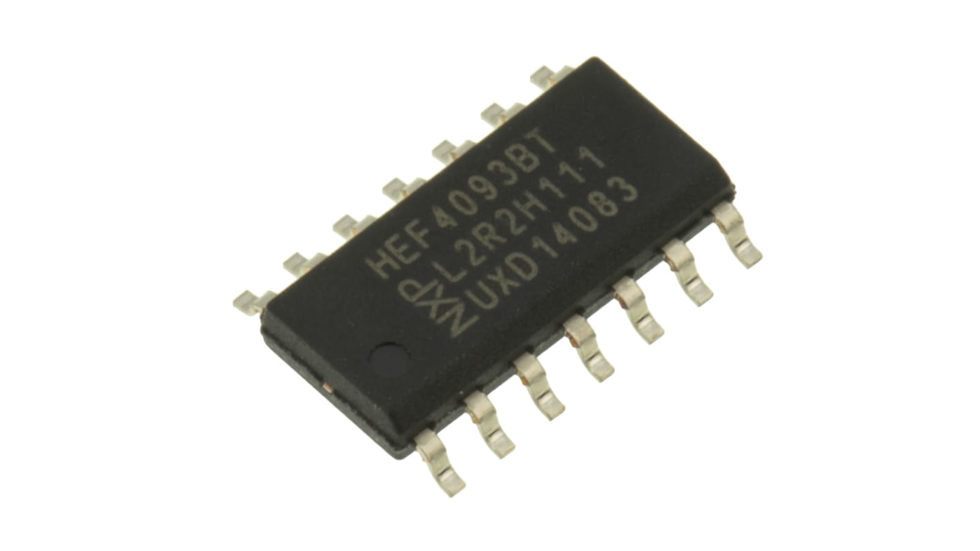
This image is representative of the product range
Bulk discount available
View bulk pricing optionsSubtotal (1 tube of 57 units)*
SGD12.996
(exc. GST)
SGD14.193
(inc. GST)
FREE delivery for orders over $150, or create a business account to enjoy free delivery from just $28
Last RS stock
- 1,881 left, ready to ship from another location
- Final 9,633 unit(s) shipping from 22 July 2026
Units | Per unit | Per Tube* |
|---|---|---|
| 57 - 57 | SGD0.228 | SGD13.00 |
| 114 - 228 | SGD0.216 | SGD12.31 |
| 285 - 513 | SGD0.205 | SGD11.69 |
| 570 - 1083 | SGD0.195 | SGD11.12 |
| 1140 + | SGD0.185 | SGD10.55 |
*price indicative
- RS Stock No.:
- 124-2313
- Mfr. Part No.:
- HEF4093BT,652
- Manufacturer:
- Nexperia
Specifications
Technical data sheets
Legislation and Compliance
Product Details
Find similar products by selecting one or more attributes.
Select all | Attribute | Value |
|---|---|---|
| Brand | Nexperia | |
| Logic Function | NAND | |
| Product Type | Logic Gate | |
| Mount Type | Surface | |
| Number of Elements | 4 | |
| Number of Inputs per Gate | 2 | |
| Schmitt Trigger Input | Yes | |
| Package Type | SOIC | |
| Pin Count | 14 | |
| Logic Family | 4000 | |
| Input Type | Schmitt Trigger | |
| Minimum Operating Temperature | -40°C | |
| Maximum Propagation Delay Time @ CL | 185ns | |
| Maximum High Level Output Current | -4.2mA | |
| Maximum Operating Temperature | 125°C | |
| Height | 1.45mm | |
| Series | HEF4093B | |
| Minimum Supply Voltage | 3V | |
| Standards/Approvals | JEDEC JESD 13-B | |
| Length | 8.75mm | |
| Maximum Supply Voltage | 15V | |
| Maximum Low Level Output Current | 4.2mA | |
| Automotive Standard | No | |
| Select all | ||
|---|---|---|
Brand Nexperia | ||
Logic Function NAND | ||
Product Type Logic Gate | ||
Mount Type Surface | ||
Number of Elements 4 | ||
Number of Inputs per Gate 2 | ||
Schmitt Trigger Input Yes | ||
Package Type SOIC | ||
Pin Count 14 | ||
Logic Family 4000 | ||
Input Type Schmitt Trigger | ||
Minimum Operating Temperature -40°C | ||
Maximum Propagation Delay Time @ CL 185ns | ||
Maximum High Level Output Current -4.2mA | ||
Maximum Operating Temperature 125°C | ||
Height 1.45mm | ||
Series HEF4093B | ||
Minimum Supply Voltage 3V | ||
Standards/Approvals JEDEC JESD 13-B | ||
Length 8.75mm | ||
Maximum Supply Voltage 15V | ||
Maximum Low Level Output Current 4.2mA | ||
Automotive Standard No | ||
- COO (Country of Origin):
- TH
The HEF4093B is a quad two-input NAND gate. Each input has a Schmitt trigger circuit. The gate switches at different points for positive-going and negative-going signals. The difference between the positive voltage (VT+) and the negative voltage (VT-) is defined as hysteresis voltage (VH). It operates over a recommended VDD power supply range of 3 V to 15 V referenced to VSS (usually ground). Unused inputs must be connected to VDD, VSS, or another input.
Key features and benefits
Mixed 5 V and 3.3 V applications
Reduce time to market for complex designs
Save board space
Open-drain output options
Improved signal integrity for complex layouts
Wide supply voltage range
Low propagation delay
Overvoltage tolerant options
Low input threshold options
CMOS low power
Related links
- Nexperia HEF4093BT 4 2-Input NAND Schmitt Trigger Input Logic Gate, 14-Pin SO
- Nexperia 74HCT132D 4 2-Input NAND Schmitt Trigger Input Logic Gate, 14-Pin SOIC
- onsemi 14-Pin SOIC
- Texas Instruments CD4093BF 14-Pin CDIP
- DiodesZetex 14-Pin TSSOP
- DiodesZetex 74HCT00S14-13 14-Pin SOIC
- onsemi MC14093BDR2G 14-Pin SOIC
- onsemi MC14093BDG 14-Pin SOIC