Nexperia 74LVC2G07GW,125 2-Channel Buffer & Line Driver, Open Drain, Non-Inverting, 6-Pin TSSOP
- RS Stock No.:
- 182-1870
- Mfr. Part No.:
- 74LVC2G07GW,125
- Manufacturer:
- Nexperia

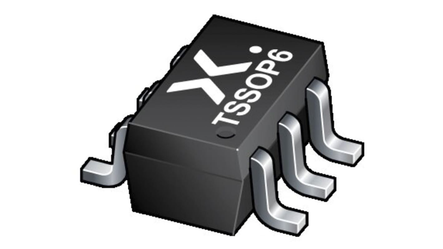
This image is representative of the product range
Bulk discount available
View bulk pricing optionsSubtotal (1 pack of 20 units)*
SGD2.86
(exc. GST)
SGD3.12
(inc. GST)
FREE delivery for orders over $150, or create a business account to enjoy free delivery from just $28
Temporarily out of stock
- Shipping from 02 September 2026
Need more? Click ‘Check delivery dates’ to find extra stock and lead times.
Units | Per unit | Per Pack* |
|---|---|---|
| 20 - 80 | SGD0.143 | SGD2.86 |
| 100 - 480 | SGD0.14 | SGD2.80 |
| 500 - 980 | SGD0.136 | SGD2.72 |
| 1000 - 1980 | SGD0.131 | SGD2.62 |
| 2000 + | SGD0.127 | SGD2.54 |
*price indicative
- RS Stock No.:
- 182-1870
- Mfr. Part No.:
- 74LVC2G07GW,125
- Manufacturer:
- Nexperia
Specifications
Technical data sheets
Legislation and Compliance
Product Details
Find similar products by selecting one or more attributes.
Select all | Attribute | Value |
|---|---|---|
| Brand | Nexperia | |
| Logic Family | 74LVC | |
| Product Type | Buffer & Line Driver | |
| Logic Function | Buffer | |
| IC Type | Buffer & Line Driver IC | |
| Number of Channels | 2 | |
| Input Type | Schmitt Trigger | |
| Output Type | Open Drain | |
| Polarity | Non-Inverting | |
| Mount Type | Surface | |
| Package Type | TSSOP | |
| Pin Count | 6 | |
| Minimum Supply Voltage | 1.65V | |
| Maximum Supply Voltage | 5.5V | |
| Maximum Propagation Delay Time @ CL | 3.7ns | |
| Maximum Low Level Output Current | 32mA | |
| Minimum Operating Temperature | -40°C | |
| Maximum Operating Temperature | 125°C | |
| Length | 2.2mm | |
| Standards/Approvals | No | |
| Series | 74LVC2G07 | |
| Height | 1.1mm | |
| Supply Current | 4μA | |
| Automotive Standard | No | |
| Select all | ||
|---|---|---|
Brand Nexperia | ||
Logic Family 74LVC | ||
Product Type Buffer & Line Driver | ||
Logic Function Buffer | ||
IC Type Buffer & Line Driver IC | ||
Number of Channels 2 | ||
Input Type Schmitt Trigger | ||
Output Type Open Drain | ||
Polarity Non-Inverting | ||
Mount Type Surface | ||
Package Type TSSOP | ||
Pin Count 6 | ||
Minimum Supply Voltage 1.65V | ||
Maximum Supply Voltage 5.5V | ||
Maximum Propagation Delay Time @ CL 3.7ns | ||
Maximum Low Level Output Current 32mA | ||
Minimum Operating Temperature -40°C | ||
Maximum Operating Temperature 125°C | ||
Length 2.2mm | ||
Standards/Approvals No | ||
Series 74LVC2G07 | ||
Height 1.1mm | ||
Supply Current 4μA | ||
Automotive Standard No | ||
- COO (Country of Origin):
- MY
The 74LVC2G07 provides two non-inverting buffers. The output of this device is an open drain and can be connected to other open-drain outputs to implement active-LOW wired-OR or active-HIGH wired-AND functions. Inputs can be driven from either 3.3 V or 5 V devices. This feature allows the use of this device in a mixed 3.3 V and 5 V environment. Schmitt trigger action at all inputs makes the circuit tolerant for slower input rise and fall time. This device is fully specified for partial power-down applications using IOFF. The IOFF circuitry disables the output, preventing the damaging backflow current through the device when it is powered down.
Wide supply voltage range from 1.65 V to 5.5 V
5 V tolerant input/output for interfacing with 5 V logic
High noise immunity
CMOS low power consumption
Latch-up performance exceeds 250 mA
Direct interface with TTL levels
Inputs accept voltages up to 5 V
Multiple package options
Specified from -40 °C to +85 °C and -40 °C to +125 °C
Related links
- Nexperia 2-Channel Buffer & Line Driver Non-Inverting, 6-Pin TSSOP
- Texas Instruments SN74LVC2G07DBVR 2-Channel Buffer & Line Driver Non-Inverting, 6-Pin SOT-23
- DiodesZetex 74LVC2G07DW-7 2-Channel Buffer & Line Driver Non-Inverting, 6-Pin SOT-363
- Texas Instruments 2-Channel Buffer & Line Driver Non-Inverting, 6-Pin SOT-23
- DiodesZetex 2-Channel Buffer & Line Driver Non-Inverting, 6-Pin SOT-363
- Nexperia 74LVC07APW Open Drain 14-Pin TSSOP
- Nexperia 74LVC07APW Open Drain 14-Pin TSSOP
- Nexperia 6-Channel Buffer & Line Driver Non-Inverting, 14-Pin TSSOP