Renesas Electronics QS3125S1G, Bus Switch, 1 x 1:1, 16-Pin
- RS Stock No.:
- 254-5004
- Mfr. Part No.:
- QS3125S1G
- Manufacturer:
- Renesas Electronics

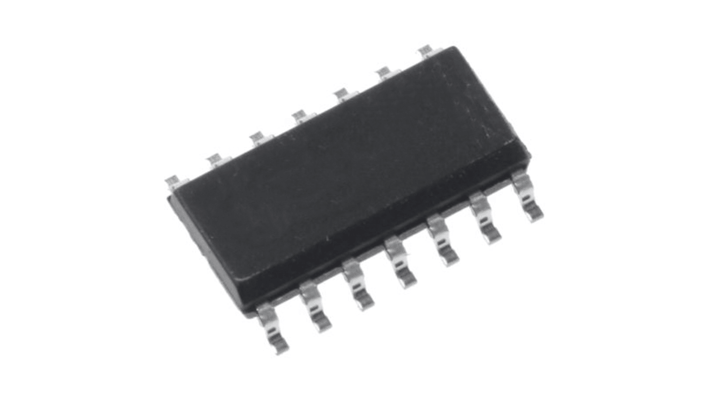
This image is representative of the product range
Currently unavailable
We don't know if this item will be back in stock, RS intend to remove it from our range soon.
- RS Stock No.:
- 254-5004
- Mfr. Part No.:
- QS3125S1G
- Manufacturer:
- Renesas Electronics
Specifications
Technical data sheets
Legislation and Compliance
Product Details
Find similar products by selecting one or more attributes.
Select all | Attribute | Value |
|---|---|---|
| Brand | Renesas Electronics | |
| Product Type | Bus Switch | |
| Logic Family | CMOS | |
| Configuration | 1 x 1:1 | |
| Number of Elements per Chip | 4 | |
| Maximum Quiescent Current | 3μA | |
| Minimum Supply Voltage | 3.3V | |
| Pin Count | 16 | |
| Maximum Supply Voltage | 5V | |
| Maximum Propagation Delay Time @ CL | 0.25ns | |
| Maximum On State Resistance | 15Ω | |
| Maximum High Level Output Current | 120mA | |
| Minimum Operating Temperature | -65°C | |
| Maximum Operating Temperature | 150°C | |
| Maximum Low Level Output Current | 120mA | |
| Standards/Approvals | RoHS | |
| Series | QS | |
| Automotive Standard | No | |
| Select all | ||
|---|---|---|
Brand Renesas Electronics | ||
Product Type Bus Switch | ||
Logic Family CMOS | ||
Configuration 1 x 1:1 | ||
Number of Elements per Chip 4 | ||
Maximum Quiescent Current 3μA | ||
Minimum Supply Voltage 3.3V | ||
Pin Count 16 | ||
Maximum Supply Voltage 5V | ||
Maximum Propagation Delay Time @ CL 0.25ns | ||
Maximum On State Resistance 15Ω | ||
Maximum High Level Output Current 120mA | ||
Minimum Operating Temperature -65°C | ||
Maximum Operating Temperature 150°C | ||
Maximum Low Level Output Current 120mA | ||
Standards/Approvals RoHS | ||
Series QS | ||
Automotive Standard No | ||
The Renesas Electronics quadruple bus switch, high-speed low resistance CMOS switches connecting inputs to outputs without propagation delay and without generating additional ground bounce noise. Individual enables (OE) are used to turn on the switches. It is Ideal for signal and control switching since the device adds no noise, ground bounce, propagation delay, or significant power consumption to the system. It can also be used for analog switching applications such as video. Quick switch devices provide an order of magnitude Faster speed than conventional logic devices. It is characterized for operation at -40°C to +85°C.
Enhanced N channel FET with no inherent diode to Vcc
Pin compatible with the 74’125 function
Zero propagation delay, zero added ground bounce
Undershoot clamp diodes on all switch and control inputs
Available in QSOP and SOIC packages